The variety of transistors inside a chip provides you an concept of how highly effective and/or energy-efficient stated chip is. An instance I like to make use of includes Apple’s A-series software processor (AP) used to energy the iPhone. The A13 Bionic AP that powered the iPhone 11 collection was constructed by TSMC utilizing its 7nm course of node and got here loaded with 8.5 billion transistors. Final 12 months’s 3nm A17 Professional AP, used to energy the iPhone 15 Professional and iPhone 15 Professional Max, carries 19 billion transistors.
We already know that MediaTek’s subsequent flagship AP, the Dimensity 9400, goes to be a powerhouse with a configuration that options one Cortex-X5 Prime CPU core, 4 Cortex-X4 Prime CPU cores, and 4 Cortex-A720 efficiency CPU cores. As soon as once more, there are not any low-power effectivity cores. Two separate “X” subscribers, @faridofanani96 and @negativeonehero have despatched tweets (by way of Wccftech) giving us some information in regards to the Dimensity 9400 SoC.
In accordance with @faridofanani96, the Dimensity 9400 AP will measure 150mm² making it the biggest chipset earmarked for a smartphone when it’s launched later this 12 months. This may enable the SoC to hold a lot of transistors together with a much bigger Neural Processing Unit (NPU) for AI and Machine Studying. Cache sizes can even be bigger and the Dimensity 9400 AP might be geared up with greater than 30 billion transistors.
MediaTek’s Dimensity 9300 AP powers the Vivo X100 collection
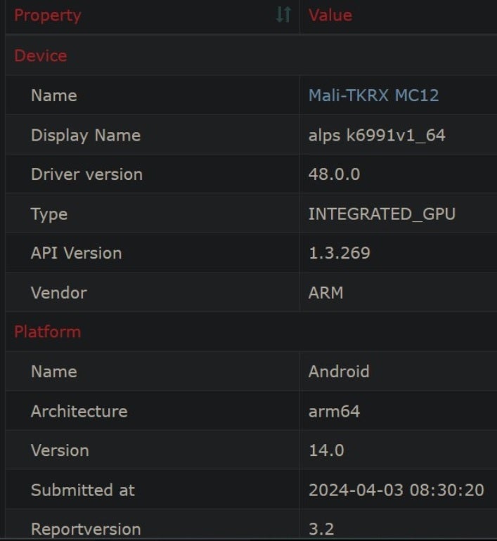
The tweet from @negativeonehero exhibits a picture from the Vulkan GPUInfo database supposedly exhibiting that the Dimensity 9400 SoC will characteristic the Mali-TKRX MC12 GPU. One rumor requires a 20% efficiency hike in graphics over the Dimensity 9300 SoC which might be sufficient for MediaTek’s new flagship smartphone chip to high the graphics efficiency of the upcoming Snapdragon 8 Gen 4 chipset.
This screenshot from the Vulkan GPUInfo database reportedly exhibits the GPU that the Dimensity 9400 SoC will characteristic
TSMC can be manufacturing the Dimensity 9400 AP utilizing its second-generation 3nm node (N3E) and all issues thought of, it will in all probability be the costliest smartphone chipset ever designed by MediaTek.
Identical to final 12 months when there have been rumors in regards to the Dimensity 9300 overheating, there was some discuss in regards to the Cortex-X5 Prime CPU core having some temperature points. One principle is that MediaTek elevated the scale of the chip’s die as a approach to cope with this situation.

